
Company Profile
| Company Name | SEISHO PWB Design Office, Ltd. (SEISHO KAIRO SEKKEI) |
|---|---|
| Established | October 1, 1991 |
| Address | 028-3606 6-54 Tsuchihashi, Yahaba, Shiwa-gun, Iwate, Japan |
| TEL | +81-19-697-8608 |
| FAX | +81-19-698-1063 |
| Capital | JPY 3,000,000 |
| President & Representative Director | Shu Hosokawa |
| Fiscal Year-End | September |
| Bank | The Bank of Iwate, Yahaba Branch |
| Website | https://www.sei-pwb.com/ |
| Business Activities |
1. Printed Circuit Board Design Single-sided, double-sided, multilayer, and flexible PCBs Transmission line simulation Power integrity simulation 2. PCB Fabrication Single-sided, double-sided, multilayer, and flexible PCBs 3. Schematic Capture 4. Electronic Component Assembly Component assembly on printed circuit boards 5. Prototyping, Design, and Evaluation of Industrial and Information Equipment Development of training materials, cybersecurity assessments, and related support |
History
SEISHO PWB Design Office was established.
Began business with local system integrators, major electrical manufacturers, and major manufacturing plants.
Introduced CR-3000 CAD for printed circuit board design.
Introduced the NIFTY online service and began transmitting design data electronically.
Obtained the Level 1 Certified Skilled Worker qualification in printed circuit board design.
Began business with a major electrical manufacturer in the optical equipment field.
Introduced CR-5000 PWS for printed circuit board design.
Began business with a major electrical manufacturer in the mobile phone field.
Moved to a new office building.
Established an in-house email environment.
Launched the company website.
Introduced CR-5000 Board Designer for printed circuit board design.
Expanded into high-frequency PCB layout design.
Introduced the CR-5000 System Designer schematic design system.
Introduced an in-house file server.
Expanded business to medical measuring instruments, environmental measurement systems, and automated production inspection equipment.
Introduced a dedicated fiber-optic connection.
Built extensive experience in high-speed signal PCB design including DDR2, PCI Express, SATA 2.0, and Gigabit Ethernet.
Exhibited for the first time at the 13th Mechanical Components & Technology Expo.
A company profile was published in Monthly Sangyo Joho Iwate, Vol. 92.
Expanded business with a major electrical manufacturer in LED lighting equipment.
Exhibited for the first time at JPCA Show 2012.
Introduced CR-8000 Design Force for printed circuit board design.
Started industrial cybersecurity-related services.
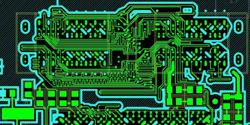
Equipment & Design Environment
- CR-8000 Design Force — 1 system
- CR-5000 Board Designer — 2 systems
- CR-5000 PWS — 5 systems
- CR-5000 System Designer — 1 system
- UltiMaker S3 — 1 unit
Access
Location
028-3606
6-54 Tsuchihashi, Yahaba, Shiwa-gun, Iwate, Japan
View larger map on Google Maps
🚗 Access
Approx. 10 minutes by car from JR Yahaba Station
Approx. 15 minutes by car from Shiwa IC on the Tohoku Expressway
🚙 Parking
Parking is available.
Please contact us in advance before visiting.